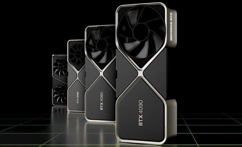
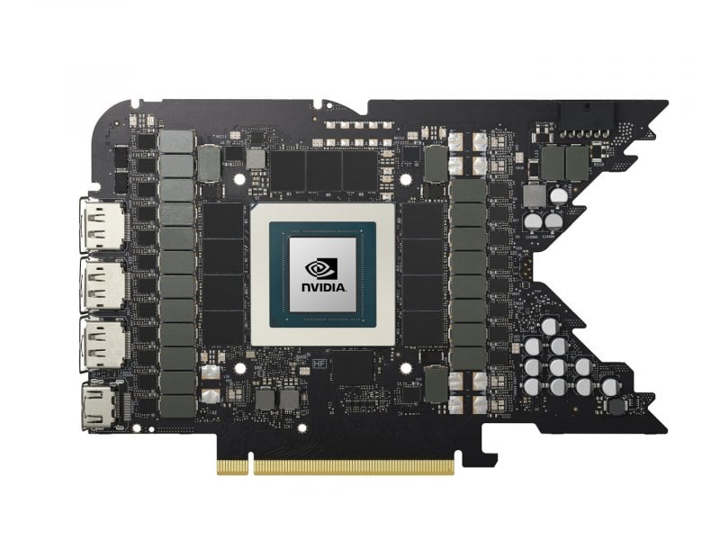
New rumors about the next NVIDIA flagship of the “Blackwell” series, the video card could have a completely revised PCB and a 512-bit interface.
New rumors about the next top of the range from the green house. According to rumors, the new NVIDIA GeForce RTX 5090 it could bring with it a completely revised design, complete with a new PCB, as well as GDDR7 memories with a 512-bit interface.
Although we are still in the field of speculation, some details are becoming more and more insistent and give a minimum of credibility to the information available. Let’s try to clarify.
New PCB, GDDR7 memories and 512-bit interface
The indiscretion comes from Panzerlied, directly from the Chiphell forum: the insider has been on the scene for some time and has often spoken about different aspects of NVIDIA’s GeForce RTX 50 “Blackwell” GPUs.
In this specific case, the leaker stated that NVIDIA’s GeForce RTX 5090 GPU will be characterized by a very dense memory layout. Notably, if the rumors are confirmed, it would be the densest design we’ve seen in recent years, given that most high-end graphics cards have resorted to maximum 384-bit memory interfaces. NVIDIA GeForce RTX 5090 should instead take a step forward and bring back 512 bits.
There should therefore be a total of 16 DRAM modules on the PCB of the RTX 5090. All these modules will be based on the GDDR7 standard and the dies, at least initially, will reach speeds of 28 Gbps. The GPU will have four memory modules on the top, five on the sides, and two on the bottom. This new configuration will require a completely new PCB design, capable of accommodating the greatest number of modules.
3 layer PCB?
According to rumors, the GeForce RTX 5090 Founders Edition could use three separate PCBs. It’s unclear whether these are three individual PCBs within a single board or three unique designs of which only one will come to life.
The cooling system will feature a double fan to calm the heat generated by the GPU and memories.
Kopite7kimi provided new details on the 3-layer PCB design: FE models are expected to feature a main PCB along with a hard IO board, accompanied by a third board that houses the PCIe connection.
In short, the new design could be more credible than one could imagine. All that remains is to wait for the official announcements from NVIDIA.
#NVIDIA #GeForce #RTX #completely #redesigned #PCB #512bit #interface #rumors

